Samsung will make the base dies for NVIDIA‘s custom high-bandwidth memory (HBM) on TSMC’s 3nm process – details of which are available in our previous report. NVIDIA asked its three suppliers for that memory (Samsung, SK hynix and Micron) to do the same, the paper says. It would be the first time Samsung has worked with TSMC at the HBM manufacturing stage.
A base die is the one chip in an HBM stack that doesn’t store your data. It’s also where NVIDIA now wants its own circuitry, built by a logic foundry.
What HBM is
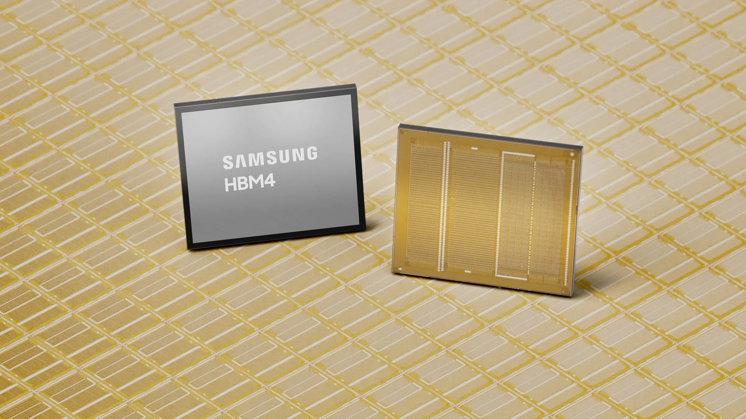
HBM is DRAM built upward. Samsung’s HBM page describes it as several memory dies stacked vertically and connected through through-silicon vias (TSVs), in a package of around 1–2 cm² and about 1mm thick. TSVs are electrodes that pass straight down through the chips, and a stack can have thousands of them, SK hynix says.
The stack sits right beside the processor. In TSMC’s CoWoS packaging, the GPU or custom AI chip and the HBM share a special substrate called an interposer, SK hynix explains. NVIDIA’s technical post puts the reason in one line: HBM “places vital memory bandwidth close to the accelerator.”
The connection is extremely wide. Samsung’s HBM4 doubles its data connections from 1,024 to 2,048 pins, and each stack moves up to 3.3 terabytes a second, 2.7 times its HBM3E, Samsung says.
What the base die does
The base die is the bottom layer, and it’s the one wired to the processor. SK hynix’s announcement of its TSMC partnership says HBM is made by stacking DRAM dies on a base die, and the base die is connected to the GPU, which controls the HBM.
It’s a different kind of chip from the layers above it. SK hynix calls it the “base logic chip”, and Seoul Economic Daily calls it a system semiconductor, while the DRAM layers are the memory.
Memory makers have built it themselves. SK hynix used its own technology for base dies up to HBM3E. Samsung has made both the DRAM layers and the base die for all of its HBM, and its HBM4 uses a 4nm logic base die from its own foundry.
Why NVIDIA wants its controller down there
Today, the circuitry that runs the memory sits on the processor. “Traditional HBM architectures place the memory controller on the XPU die, consuming valuable silicon area that could otherwise be dedicated to compute,” NVIDIA says. XPUs are custom AI accelerators, in NVIDIA’s terms.
On August 26th, NVIDIA announced NVHBM, which moves its own memory controller into the base die instead. Standard HBM relies on wider interface connections, and the custom base die shrinks the physical memory interface (PHY) and support area by up to 67%, NVIDIA’s technical post says.
NVIDIA’s claims, all against standard HBM4E: up to 30% more memory bandwidth per stack, 15% lower HBM power and up to 25% more area on the compute die for other features. In a 1-gigawatt data center running 2,000W chips, NVIDIA says, the power savings leave room for up to 15,000 more of them.
NVHBM is offered through NVLink Fusion, which lets other companies plug their own AI chips into NVIDIA’s rack-scale platform, with Amazon’s Annapurna Labs first in line. NVIDIA says the technology is the same one it will use for its own future GPUs.
Why TSMC is now part of making memory
The base die was always logic, and logic is TSMC’s business. SK hynix calls TSMC “a top global logic foundry”, and it moved its HBM4 base die to TSMC’s logic process “so additional functionality can be packed into limited space.”
In April, SK hynix showed a 16-layer, 48GB HBM4 labeled “Powered by base die in TSMC advanced logic”, its post from TSMC’s symposium says. TSMC’s own post from its 2025 Open Innovation Platform Forum names its N12 process for HBM4 base dies and N3P for custom HBM4E.
NVIDIA wants one base die from every supplier. It asked for NVHBM base dies on TSMC’s 3nm and DRAM layers on the sixth-generation 1c process, because different manufacturing methods make it hard to get consistent performance from one design, the report says. NVIDIA says a standard NVHBM design also cuts the work of qualifying memory from several suppliers.
Samsung is the odd one out, since it runs its own foundry. It agreed after an internal review, the report says, but keeps doing everything in-house for standard HBM and for other customers’ custom HBM, including AMD’s. It’s also checking whether its own foundry can make NVHBM base dies, which an industry official calls a hedge in case demand outruns TSMC’s capacity.
What it means for the memory crunch
Moving the base die doesn’t change who makes the memory itself. Samsung’s DRAM layers for HBM4 and HBM4E come off 1c lines at its Hwaseong and Pyeongtaek campuses, the report says.
AI servers are still pulling memory supply away from PCs and phones. TrendForce says DRAM makers keep prioritizing their advanced capacity for server products, with conventional DRAM contract prices set to rise 10–15% in the fourth quarter and PC memory supply possibly shrinking in 2027. Our memory crunch explainer has what that means for laptop buyers.
The take
With NVHBM, NVIDIA designs the controller in the bottom chip, and if the report’s right, it also picks the factory and the DRAM process its suppliers use. That’s a lot of control over a part NVIDIA doesn’t make, and we think it’s where AI memory is headed: SK hynix says it will move beyond standardized HBM to custom HBM tailored to specific customer requirements. Samsung’s own schedule has custom HBM samples reaching customers in 2027.